We love using our gadgets, you know when they are actually fully assembled and functioning, but we also have a bizarre affinity to watching them get torn down into dozens of separate parts giving us a glimpse of what’s inside.
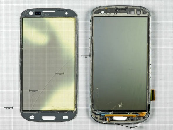
The latest device to have received the teardown treatment is none other than the hero smartphone of the moment, the Samsung Galaxy S III. As usual the good folks over at iFixit did the slicing and dicing, which has revealed a number of tasty bites.
First off, the Galaxy S III is surprisingly easy to open, with a number of standard Phillips screws holding it together. Inside you will find the motherboard assembly, the 4.8-inch PenTile Matrix Super AMOLED display (be sure to check out our comparison between PenTile Matrix Super AMOLED and standard RGB LCD display technologies) that is optically laminated to the Gorilla Glass 2 fortified glass and the 8-megapixel rear camera assembly.
You might want to know that for the camera, Samsung has opted for a Sony backside-illuminated CMOS sensor, similar to the one used in the iPhone 4S and Xperia Arc.
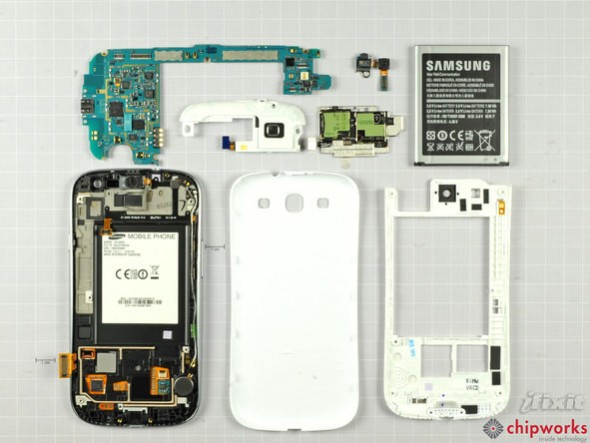
Other parts include:
- Samsung Exynos 4412 quad-core A9 SoC with 1 GB LP DDR2 Green Memory (K3PE7E700M-XGC2)
- Murata M2322007 WiFi Module
- Samsung KMVTU000LM eMMC(16GB)+MDDR(64MB) NAND Flash
- Intel Wireless PMB9811X Gold Baseband processor
- Broadcom BCM47511 Integrated Monolithic GNSS Receiver
- Wolfson Microelectronics WM1811 stereo codec
- Skyworks SKY77604 Multi-Band Power amplifier
- Silicon Image 9244 low-power MHL Transmitter
- NXP PN544 NFC Chip
- Infineon PMB5712 RF transceiver
Now we’re certainly impressed.
[iFixit]
